- 您现在的位置:买卖IC网 > Sheet目录3881 > PIC18F4539T-E/ML (Microchip Technology)IC PIC MCU FLASH 12KX16 44QFN
PIC18FXX39
DS30485A-page 44
Preliminary
2002 Microchip Technology Inc.
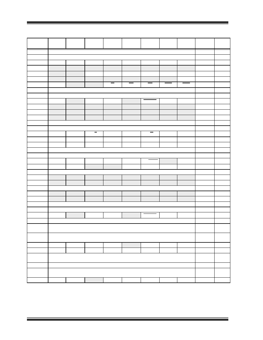
TMR0H
Timer0 Register High Byte
0000 0000
TMR0L
Timer0 Register Low Byte
xxxx xxxx
T0CON
TMR0ON
T08BIT
T0CS
T0SE
PSA
T0PS2
T0PS1
T0PS0
1111 1111
OSCCON*
—
*
---- ---0
LVDCON
—
IRVST
LVDEN
LVDL3
LVDL2
LVDL1
LVDL0
--00 0101
WDTCON
—
—SWDTE
---- ---0
RCON
IPEN
—
—RI
TO
PD
POR
BOR
0--1 11qq
TMR1H
Timer1 Register High Byte
xxxx xxxx
TMR1L
Timer1 Register Low Byte
xxxx xxxx
T1CON
RD16
—
T1CKPS1
T1CKPS0
—
T1SYNC
TMR1CS
TMR2*
*
0000 0000
PR2*
*
1111 1111
T2CON*
*
-000 0000
SSPBUF
SSP Receive Buffer/Transmit Register
xxxx xxxx
SSPADD
SSP Address Register in I2C Slave mode. SSP Baud Rate Reload Register in I2C Master mode.
0000 0000
SSPSTAT
SMP
CKE
D/A
PS
R/W
UA
BF
0000 0000
SSPCON1
WCOL
SSPOV
SSPEN
CKP
SSPM3
SSPM2
SSPM1
SSPM0
0000 0000
SSPCON2
GCEN
ACKSTAT
ACKDT
ACKEN
RCEN
PEN
RSEN
SEN
0000 0000
ADRESH
A/D Result Register High Byte
xxxx xxxx
ADRESL
A/D Result Register Low Byte
xxxx xxxx
ADCON0
ADCS1
ADCS0
CHS2
CHS1
CHS0
GO/DONE
—ADON
0000 00-0
ADCON1
ADFM
ADCS2
—
PCFG3
PCFG2
PCFG1
PCFG0
00-- 0000
CCPR1H
PWM Register1 High Byte (Read only)
xxxx xxxx
CCPR1L*
*
xxxx xxxx
CCP1CON*
—
*
--00 0000
CCPR2H
PWM Register2 High Byte (Read only)
xxxx xxxx
CCPR2L*
*
xxxx xxxx
CCP2CON*
—
*
--00 0000
TMR3H
Timer3 Register High Byte
xxxx xxxx
TMR3L
Timer3 Register Low Byte
xxxx xxxx
T3CON
RD16
—
T3CKPS1
T3CKPS0
—
T3SYNC
TMR3CS
SPBRG
USART1 Baud Rate Generator
0000 0000
RCREG
USART1 Receive Register
0000 0000
TXREG
USART1 Transmit Register
0000 0000
TXSTA
CSRC
TX9
TXEN
SYNC
—
BRGH
TRMT
TX9D
0000 -010
RCSTA
SPEN
RX9
SREN
CREN
ADDEN
FERR
OERR
RX9D
0000 000x
EEADR
Data EEPROM Address Register
0000 0000
EEDATA
Data EEPROM Data Register
0000 0000
EECON2
Data EEPROM Control Register 2 (not a physical register)
---- ----
EECON1
EEPGD
CFGS
—
FREE
WRERR
WREN
WR
RD
xx-0 x000
TABLE 4-2:
REGISTER FILE SUMMARY (CONTINUED)
File Name
Bit 7
Bit 6
Bit 5
Bit 4
Bit 3
Bit 2
Bit 1
Bit 0
Value on
POR, BOR
Details
on page:
Legend:
x
= unknown, u = unchanged, - = unimplemented, q = value depends on condition
*
These registers (or individual bits) are retained to maintain compatibility with PIC18FXX2 devices; however, the indicated bits are
reserved in PIC18FXX39 devices. Users should not alter the values of these bits. See Section 4.9.2 for details.
Note 1: RA6 and associated bits are configured as port pins in RCIO and ECIO Oscillator mode only and read '0' in all other Oscillator modes.
2: Bit 21 of the TBLPTRU allows access to the device configuration bits.
3: These registers and bits are reserved on the PIC18F2X39 devices; always maintain these clear.
发布紧急采购,3分钟左右您将得到回复。
相关PDF资料
PIC18LF8680T-I/PT
IC PIC MCU FLASH 32KX16 80TQFP
PIC16F1936-I/SO
IC PIC MCU FLASH 512KX14 28-SOIC
PIC18F24K20-I/SO
IC PIC MCU FLASH 8KX16 28SOIC
PIC18LF8585T-I/PT
IC PIC MCU FLASH 24KX16 80TQFP
XF2J-3024-11
CONN FPC 30POS 0.5MM SMT
PIC18LF6525T-I/PT
IC PIC MCU FLASH 24KX16 64TQFP
PIC18LF8621T-I/PT
IC PIC MCU FLASH 32KX16 80TQFP
PIC18F8620T-E/PT
IC PIC MCU FLASH 32KX16 80TQFP
相关代理商/技术参数
PIC18F4539T-E/PT
功能描述:8位微控制器 -MCU 24KB 1408 RAM 32 I/O RoHS:否 制造商:Silicon Labs 核心:8051 处理器系列:C8051F39x 数据总线宽度:8 bit 最大时钟频率:50 MHz 程序存储器大小:16 KB 数据 RAM 大小:1 KB 片上 ADC:Yes 工作电源电压:1.8 V to 3.6 V 工作温度范围:- 40 C to + 105 C 封装 / 箱体:QFN-20 安装风格:SMD/SMT
PIC18F4539T-I/ML
功能描述:8位微控制器 -MCU 24KB 1408 RAM 32 I/O RoHS:否 制造商:Silicon Labs 核心:8051 处理器系列:C8051F39x 数据总线宽度:8 bit 最大时钟频率:50 MHz 程序存储器大小:16 KB 数据 RAM 大小:1 KB 片上 ADC:Yes 工作电源电压:1.8 V to 3.6 V 工作温度范围:- 40 C to + 105 C 封装 / 箱体:QFN-20 安装风格:SMD/SMT
PIC18F4539T-I/PT
功能描述:8位微控制器 -MCU 24KB 1408 RAM 32 I/O RoHS:否 制造商:Silicon Labs 核心:8051 处理器系列:C8051F39x 数据总线宽度:8 bit 最大时钟频率:50 MHz 程序存储器大小:16 KB 数据 RAM 大小:1 KB 片上 ADC:Yes 工作电源电压:1.8 V to 3.6 V 工作温度范围:- 40 C to + 105 C 封装 / 箱体:QFN-20 安装风格:SMD/SMT
PIC18F4550EPT
制造商:Microchip Technology Inc 功能描述:
PIC18F4550-I/ML
功能描述:8位微控制器 -MCU 32kBF 2048RM FSUSB2 RoHS:否 制造商:Silicon Labs 核心:8051 处理器系列:C8051F39x 数据总线宽度:8 bit 最大时钟频率:50 MHz 程序存储器大小:16 KB 数据 RAM 大小:1 KB 片上 ADC:Yes 工作电源电压:1.8 V to 3.6 V 工作温度范围:- 40 C to + 105 C 封装 / 箱体:QFN-20 安装风格:SMD/SMT
PIC18F4550-I/P
功能描述:8位微控制器 -MCU 32kBF 2048RM FSUSB2 RoHS:否 制造商:Silicon Labs 核心:8051 处理器系列:C8051F39x 数据总线宽度:8 bit 最大时钟频率:50 MHz 程序存储器大小:16 KB 数据 RAM 大小:1 KB 片上 ADC:Yes 工作电源电压:1.8 V to 3.6 V 工作温度范围:- 40 C to + 105 C 封装 / 箱体:QFN-20 安装风格:SMD/SMT
PIC18F4550-I/PT
功能描述:8位微控制器 -MCU 32kBF 2048RM FSUSB2 RoHS:否 制造商:Silicon Labs 核心:8051 处理器系列:C8051F39x 数据总线宽度:8 bit 最大时钟频率:50 MHz 程序存储器大小:16 KB 数据 RAM 大小:1 KB 片上 ADC:Yes 工作电源电压:1.8 V to 3.6 V 工作温度范围:- 40 C to + 105 C 封装 / 箱体:QFN-20 安装风格:SMD/SMT
PIC18F4550T-I/ML
功能描述:8位微控制器 -MCU 32kBF 2048RM FSUSB2 RoHS:否 制造商:Silicon Labs 核心:8051 处理器系列:C8051F39x 数据总线宽度:8 bit 最大时钟频率:50 MHz 程序存储器大小:16 KB 数据 RAM 大小:1 KB 片上 ADC:Yes 工作电源电压:1.8 V to 3.6 V 工作温度范围:- 40 C to + 105 C 封装 / 箱体:QFN-20 安装风格:SMD/SMT